- upload bom file
- +86 0755-82770375
- info@onepcba.com
- Compare Products
- Change Location:
What’s The Difference Between Printed Circuit Board and Integrated Circuit Board?

What’s The Difference Between Printed Circuit Board and Integrated Circuit Board?
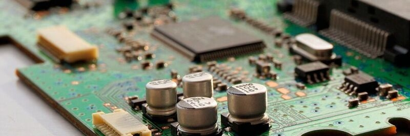
What is a printed circuit board?
Printed circuit board, also known as PCB, is the electrical connection provider of electronic components. It has a history of over 100 years. Its design is mainly layout design. The main advantages of using circuit boards are greatly reduced wiring and assembly errors and improved level of automation and production labor rate. According to the number of PCB, layers can be divided into a single board, double panel, four-layer board, six-layer board, and other multi-layer board. Let's look at printed circuit boards and integrated circuits.
Difference between PCB and integrated circuit board (IC)
An integrated circuit generally refers to an integrated chip. For example, the Northbridge chip and CPU on the motherboard are called integrated circuits. The original name is also called an ensemble block. A printed circuit refers to what we usually see as a circuit board, and the welded chips printed on the board.
The integrated circuit (IC) is welded to the PCB board; PCB is the carrier of the integrated circuit (IC). PCB is a printed circuit board. Printed circuit boards will appear in almost every kind of electronic device. If there are electronic parts in a device, a printed circuit board is embedded on a PCB of different sizes. In addition to fixing various small parts, the main function of the printed circuit board is to make an electrical connection between the above parts.
In a nutshell, an integrated circuit is the integration of a general-purpose circuit onto a chip. It's a whole thing. Once the inside is damaged, the chip will be damaged. PCBs can weld their own components. If the device is damaged, you can replace the parts.
PCB board composition
The current circuit board is mainly composed of the following parts:
Circuits and modes: Circuits are used as tools for conduction between components. In the design, a large copper surface will be designed as the ground and power layer. The routes and drawings were made at the same time.
Dielectric layer: used to maintain the insulation between the circuit and each layer, commonly known as the substrate.
Through/Through hole: Through holes allow more than two layers of wire to conduct electricity to each other. The larger through-hole is used for component insertion. In addition, non-through-hole (north) screws are commonly used for surface mount positioning and setting during assembly.
Solder/mask: Not all copper surfaces need to be tinned, so a layer of material (usually epoxy) is printed on the untinned area to isolate the tinned copper surface to avoid short circuits between non-tinned wires. According to the different processes, can be divided into green oil, red oil, and blue oil.
Legend/mark/screen: This is an unnecessary combination. Its main function is to mark the name and position frame of each component on the circuit board for easy maintenance and identification after assembly.
Surface finish: Because the copper surface is easy to oxidize in the general environment, it cannot be tinned (poor solderability), so it will be protected on the surface of the copper to be tinned. Protection methods include HASL, ENIG, silver leaching, tin leaching, and OSP. Each method has its own advantages and disadvantages, collectively known as surface treatment.
PCB characteristics
High density: Over the decades, with the improvement of integrated circuit integration and installation technology, PCB high density has been developed.
High reliability: Through a series of inspections, tests, and aging tests, PCB can work reliably for a long time (generally 20 years).
Designability: According to PCB performance requirements (electrical, physical, chemical, mechanical, etc.), PCB design can be realized by means of design standardization, standardization, etc., with a short time and high efficiency.
Producibility: With modern management, standardization, scale (quantity), automation, and other production, to ensure the consistency of product quality.
Testability: A relatively perfect test method, test standards, various test equipment, and instruments have been established to test and identify the qualification and service life of PCB products.
Assemblability: PCB products are not only convenient for the standardized assembly of various components, but also can realize automatic and large-scale mass production. At the same time, PCB and various component assembly parts can also be assembled into larger parts, systems, and even the whole machine.
Maintainability: Since the design and production of PCB products and various component assembly parts are standardized, these parts are standardized as well. Therefore, in case of system failure, the system can be replaced quickly, easily, and flexibly, and the system can be quickly restored. Of course, there are many more examples. Such as the system miniaturization, and lightweight, high-speed signal transmission.
Characteristics of integrated circuits
The integrated circuit has the advantages of small size, lightweight, less lead and solder joints, long life, high reliability, good performance, low cost, easy mass production, and so on. It is not only widely used in industrial and civil electronic equipment, such as tape recorders, television, computer, and so on, but also widely used in military, communication, remote control, and so on. Using integrated circuits to assemble electronic equipment, its assembly density is tens to thousands of times higher than that of transistors, and can greatly improve the stable working time of equipment.
An integrated circuit is a miniature electronic device or component. Transistors, resistors, capacitors, inductors, and other components required in the circuit are connected to each other through a certain process, assembled in a small piece or a few pieces of small semiconductor chips or dielectric substrate, and then packaged in the shell, forming a micro-structure with the required circuit functions; All components are integrated into the structure, making electronic components a big step forward to miniaturization, low power consumption, intelligence, and high reliability. The circuit is represented by the letter "IC". The inventors of the integrated circuit were Jack Kilby (General Electric-based integrated circuit) and Robert Noyce (silicon-based integrated circuit).
Currently, most applications in the semiconductor industry are silicon-based integrated circuits. It is a new type of semiconductor device developed in the late 1950s and 1960s. It is through oxidation, lithography, diffusion, epitaxy, aluminum evaporation, and other semiconductor manufacturing processes, the semiconductor, resistance, capacitance and other components with a certain function of the circuit and the connection line between them integrated on a small piece of silicon and then welding the electronic devices encapsulated in the shell. There are many kinds of packaging, such as round shell, flat shell, or double in-line. Integrated circuit technology includes chip manufacturing technology and design technology, mainly reflected in processing equipment, processing technology, packaging testing, mass production, and design innovation ability.