- upload bom file
- +86 0755-82770375
- info@onepcba.com
- Compare Products
- Change Location:
Overview
Essential details
| Model Number: | Customized | Place of Origin: | Guangdong, China |
| Brand Name: | Customized | Base Material: | FR4/High TG FR-4/M4/ M6/Rogers/Nelco/Isola |
| Copper Thickness: | 1 - 4 OZ | Board Thickness: | 0.2-4mm |
| Min. Hole Size: | 0.15mm | Min. Line Width: | 0.1mm |
| Min. Line Spacing: | 0.1mm | Surface Finishing: | OSP,Immersion Gold,Immersion Tin,Immersion Ag |
| Board Size: | Customized |
Supply Ability
| Supply Ability | 500 Piece/Pieces per Day |
Packaging & delivery
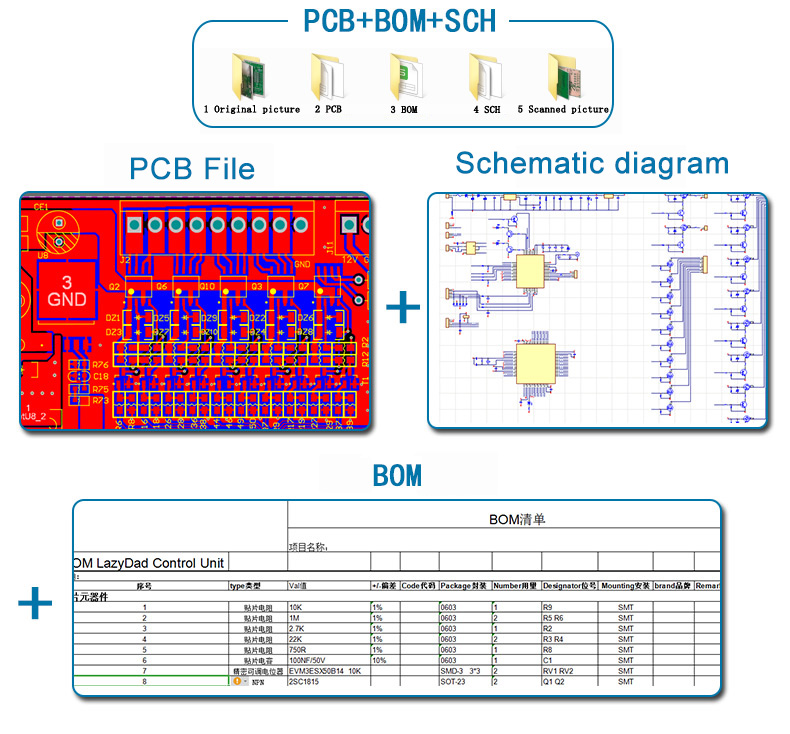
| Packaging Details | Electronic circuit board cloning:PCB file,BOM,Principle diagram PCBA:Anti-static bag packaging+Shock-proof bubble film packaging+Carton packaging | ||||||||||
| Port | shenzhen | ||||||||||
| Lead time: |
|
Video Description

How To Clone A PCB Board?
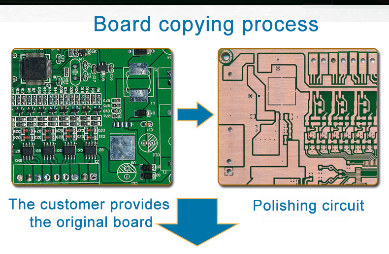
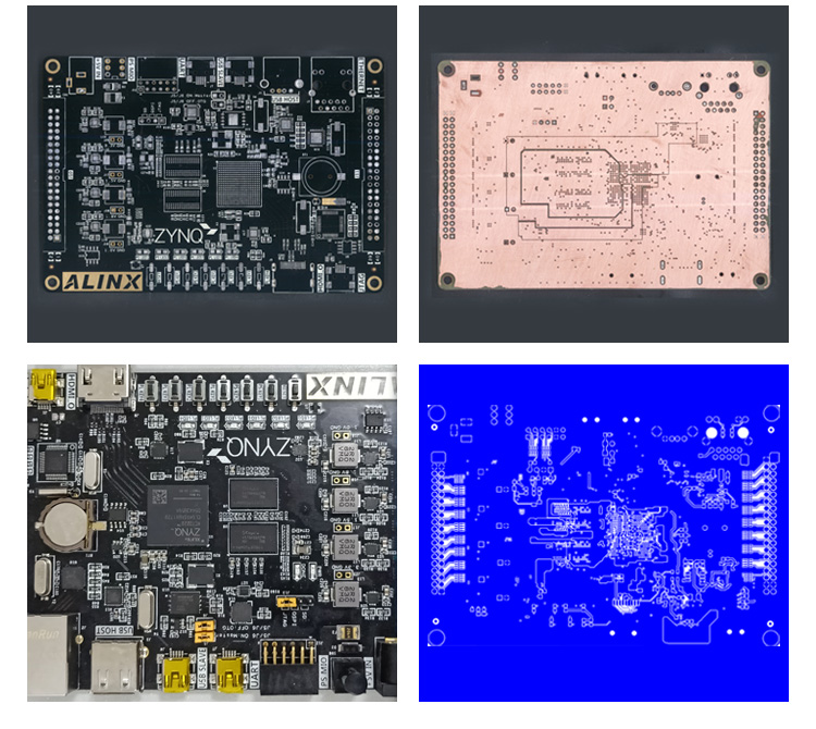
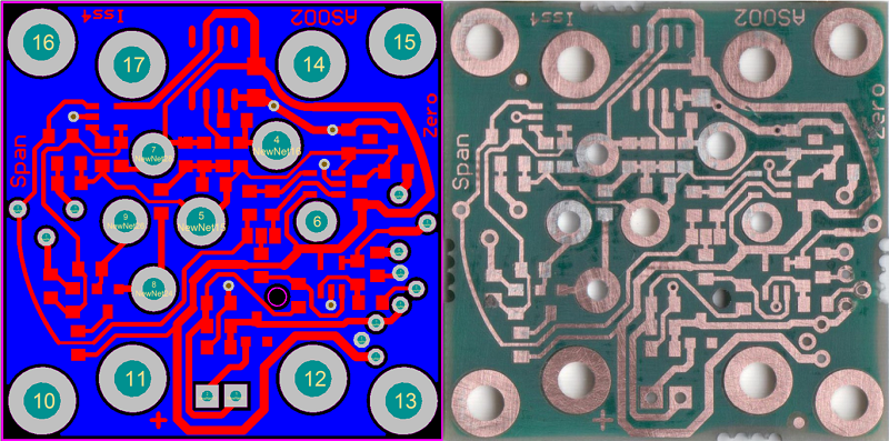
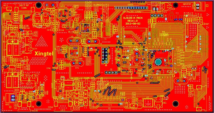
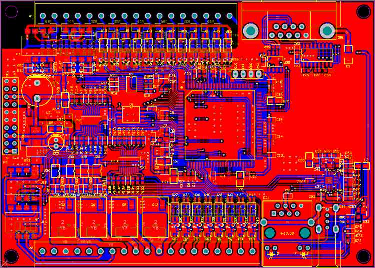
There are a few different ways to clone a printed circuit board. Each method has its own benefits and drawbacks. Make sure youunderstand the process and potential pitfalls of each method before choosing a technique. This will help you make an informeddecision and produce the desired results. Generally, we’ll clone pcbs according below procedures:
#1 - IC Unlock (Decryption)
Extract the program from Board25%
#2 - PCB Reverse Engineering
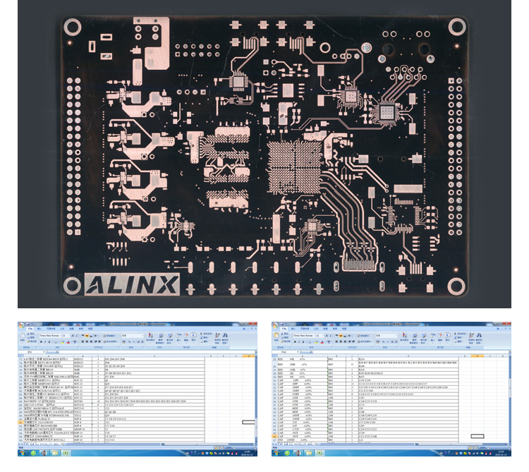
Get gerber file & BOM list, creating layout and converting it into a schematic50%
#3 - Prototype PCB Fabrication
Building and producing the pcb sample with schematic75%
#4 - PCB Functional Testing
Inspect the performance of the new board, troubleshoot issues, and fix incompatibilities before themass production100%
Tips:
For #1, IC unlock is only necessory only if your program is locked.
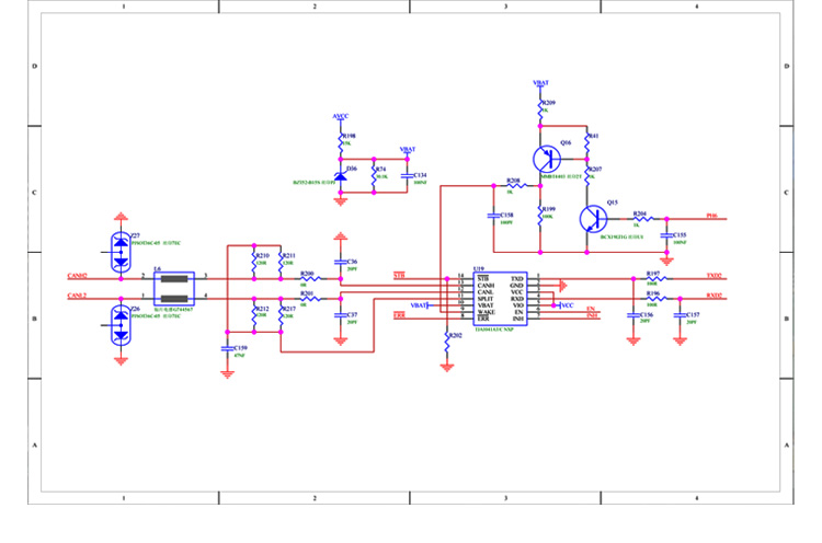
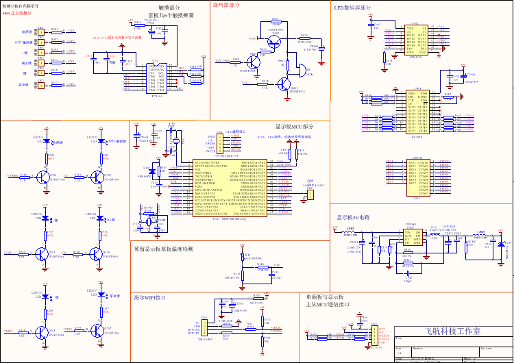
For #2, it’s the most important process. You need to get the bill of material bom and schematic diagram by using reverse engineering technology.
Required Tools And Equipment:
* Computer
* AUTOCAD
* Scanner
* PORTEL
Step 1: Scan The Original PCB
First, you must put the original PCB inside the scanner. And then, you must adjust the scanner’s contrast and brightness settings.
Step 2: Open AUTOCAD And Create A File
To begin, open AUTOCAD and create a file. From the insert menu, select raster images. Then, select the desired image for the project. The insert image box will appear. When you insert an image, draw a rectangular frame around the PCB. Use the object lock point as much as possible when building the structure to ensure tracking.
Step 3: Drawing Component Package And The Shape
To begin, create a board design by calculating the quantity of boards in the design. Every package must include one board drawing. After that, use PORTE99 to generate the electronic components package and shape.
Step 4: Put The CAD File To PRORTE99
Open the PORTEL99 PCB editor and select ‘import CAD file’ from its menu to create a new PCB file. Import the CAD file into it. Once you import it, you will see the component packaging graph in the PORTEL99 editor.
Step 5: Create Another PCB Component Editor
PROTEL99 provides a PCB component editor where you can open another one and place a component.
Step 6: Send The Component Packages To CAD File
After you have finished creating all the component packages in the PROTEL99 editor, send each one to a CAD file.
Step 7: Copy The Component Package To The CAD
Make a copy of the PCB image into the imported CAD file by duplicating the newly created CAD file’s component package. Open both CAD files.
Step 8: Put The Vias And Pads
Measure the inner, external, and internal diameters of the pads and vias, then choose the Circle sub-item from the drawing menu. After that, you must compute the ring’s inner and outer dimensions. You will not be able to place both the square and polygon pads because of this. Furthermore, you must place each pad based on its size. Fill in the CAD instead.
Step 9: Draw The Trace And Put The Silkscreen
At the end, you can use the Drawing menu to select the line aggregate. Then, you can add the silkscreen. If you want an irregular screen, you must use the polymer line.

| Item(pcb) | Capability (pcb) |
| Base Material | FR-4 / High TG FR-4 / Halogen Free material/Rogers/Arlon/Taconic/Teflon |
| Layers | 1-22 |
| copper thickness | 1-6 OZ |
| Finished board thickness | 0.2-7.0mm |
| Min hole size | Mechanical hole: 0.15mm Laser hole: 0.1mm |
| Controlled Impedance | +/-5% |
| Surface treatment | HASL, HASL lead free, Immersion Gold, Immersion Tin, Immersion Silver, Hard gold,Flash gold, OSP… |
| solder mask | green/blue/black/white/red/pink/orange/yellow |
| Plugging vias capability | 0.2-0.8mm |
| Outline profile | Rout/ V-cut/ Bridge/ Stamp hole |
Thank you for visiting our website. If you have any suggestions or comments, please leave a message to us.
We will reply to you as soon as possible. Thank you!
+86 18810662250 (skype/whatsapp)
Email:rhoda@onepcba.com
Phone: +86 18810662250


