- upload bom file
- +86 0755-82770375
- info@onepcba.com
- Compare Products
- Change Location:
PCB circuit board design sequence

PCB circuit board design sequence

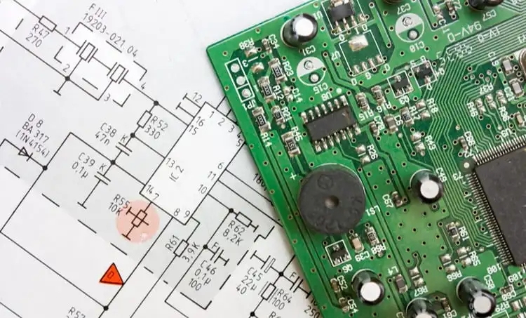
A PCB schematic is a desired design or blueprint.
In the PCB layout design phase, the designer completes the wiring and placement of components.
I used to work on a power electronics project where the control panel was connected vertically to the power circuit. Even when the controller PCB is working properly, the circuit board does not provide the desired output. After debugging, our team believes that there are some wiring errors in the power board. The results of PCB design services received from the service bureau where we outsourced work were poor. We had to redo the boards, which was a challenge and delayed the project. As a precaution, we blacklisted that particular service bureau from further projects. As we have learned, a poor PCB design service can have a negative impact on a project in many ways, as every stage of PCB design is critical to the success of the product. The following combination of my experience for you to summarize the PCB design sequence.
Order of PCB design service:
PCB design services play an important role in meeting the quality, reliability, and accuracy requirements of the electronic marketplace. There is a specific sequence in any PCB design process: PCB design services begin with the design of an electronic system architecture and end with the development of a functional prototype. Let's take a closer look at what happens during the design, layout, manufacturing, assembly, and testing phases of a PCB design.

PCB Design Stage:
PCB layout design is the first step in a PCB design service if a design schematic is provided. If not, work begins by drawing a PCB design schematic. A design schematic is a circuit diagram that represents the electrical connections between the components used in a circuit. Any CAD software can be used to draw design schematics. The layout design becomes much simpler through error-free, clutter-free design solutions.
A design schematic is a diagram of the circuit to be made. Using standard notation, PCB design schematics describe the electrical connections, the components used in the circuit, and how they are connected to each other. In a PCB schematic, you may find components and wires. The wires in the PCB schematic are replaced with traces in the PCB layout. The PCB design schematic is independent of the placement of components -- this part becomes relevant when designing the PCB layout.
PCB schematics can be developed from specifications, block diagrams, labeled schematic diagrams, or simply from verbal discussions. Regardless of the source, CAD software is essential for creating PCB schematics.
PCB Layout stage:
With the help of PCB design software, design schematics can be converted into bills of materials and PCB layout diagrams. PCB layout design must be done carefully to avoid noise effects, signal degradation or loss, interference problems, and thermal and mechanical stresses. PCB layout design includes circuit board component layout and wiring diagram. In PCB wiring design, wiring establishes electrical connections between components in a circuit through traces.
PCB design software is necessary to convert PCB schematics into PCB layouts. The PCB schematic is imported into the PCB design software to form the layout design with the footprint and mouse lines of the components. Mouse lines are automatically drawn between pads belonging to the same screen name. Rat wire reveals how different components can be attached to a track and helps designers route traces as well as create through-holes and copper castings.
In the PCB layout phase, the designer completes the wiring and component placement. Various design considerations are involved in PCB layout design, such as the number of layers, PCB stacking structure, selection of component sizes suitable for housing size, board edge spacing, trace width, and hole spacing. Designers should adhere to the PCB rules applicable to the designed circuit to establish signal integrity, power integrity, interference mitigation, thermal stability, and mechanical stability.
Once the PCB layout is in place, text or indicators such as board name, company name, version number, pin marks, switch Settings, assembly instructions, copyright, and legal information can be marked on the board. These silkscreen texts make PCB assembly, rework, and debugging easier. The file containing the completed PCB layout is then transferred to the PCB manufacturer for production.
PCB Manufacturing, assembly, and testing stages:
A good PCB layout needs to meet the requirements of signal integrity, power integrity, and electromagnetic compatibility. Simulations can be run on the PCB layout to confirm that the layout meets these requirements and to evaluate board-level limitations. An approved PCB design is the manufacturer's reference for making the PCB and can be exported in the format required by the manufacturer. In some cases, a 3D model of the PCB is created to design the shell or ensure that it works properly.
With the right design software, PCB Design Services can develop high-quality products. Leading electronics vendors rely on Cadence products to optimize power, space, and energy requirements for a wide variety of market applications.

