- upload bom file
- +86 0755-82770375
- info@onepcba.com
- Compare Products
- Change Location:
Requirements for mounting machine on PCB

Requirements for mounting machine on PCB
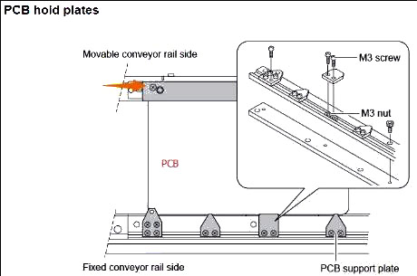
- Requirements for machine clamping edge (process edge)
Process edge: PCB edge that will be clamped when placed on the conveyor rail of the machine. The width of the plywood is 5mm (3mm on the front);
The clamping edge is required to be parallel and straight, and no component can be placed 5 mm (3 mm on the front) close to the plate edge (if not, please add the process edge);
The nonclamping edge shall not have any element protruding out of the plate;
The length of the clamping edge must be greater than 80mm, and it should be designed on the long side as far as possible, at least meeting the requirement that the clamping edge: the other side>1:1.5;
The process edge shall be added in the direction of fewer Vcuts to reduce the deformation of the plate.

The following figure does not consider the clamping edge, and the edge components may be damaged by the machine.

The process edge is added in the direction of less Vcuts to reduce deformation and avoid plate breakage


-
PCB overall dimensions and splicing
The size of PCB is 60 * 80mm-250 * 330mm, and the shape of PCB is rectangular (square). If not, please splice the board and add process edges.
The thickness of PCB is 0.8-4mm, and the maximum width thickness ratio is 150:1 (when the length of PCB is 150mm, the thickness cannot be less than 1mm);
Optimum panel size and quantity
PCB thickness is less than 1mm and there are precision components (0402, 0.5mm, and below). It is recommended that the size of the splice board be 100 * 150mm;
The thickness of PCB is less than 1mm, with precision components (0402, 0.5mm and below), and the number of splice plates does not exceed 10 * 15;
The recommended size of a conventional plate is 100 * 150-180 * 250mm.
Outline example drawing


- Positioning point requirements
Positioning point: also called datum point, the placement machine determines the position through the positioning point.
- a) There are at least 2 Fid Mark points on the surface to be pasted, and they are placed at the diagonal position
- b) Suggestions on Fid Mark's drawing method:
1mm diameter round pad+3.5mm diameter green oil windowing anti-interference+3mm diameter and 0.5mm width ring
In case of insufficient space: the Fid Mark is drawn as a 1mm round pad+2mm above resistance welding window
The outermost process ring can improve the influence of the PCB production process on the Fid Mark
When there is a splice board, the Mark point should be drawn into the board as far as possible
- c) No text or pad interference within 3mm around the Fid Mark
- d) The Fid Mark is more than 3mm away from the edge of the plate (when the process edge has 5mm, the Fid Mark is placed 3.5mm away from the edge of the plate)
- e) Bad Mark draws a 2mm round pad
The design suggested by Fid Mark: mark point+green oil window anti-interference area+process ring.


Unavailable design: The green oil window is not enlarged, and the Mark point is partially covered by the solder mask, causing the machine to be pasted away from the correct position.


-
- Design specification of bonding pad, such as meeting IPC-7351, etc.
- a) All component pins can be placed on the bonding pad
- b) The pin at the bottom of the component does not overlap with the bonding pad, and the length does not exceed 0.2mm, otherwise it is easy to short circuit or poor welding
- c) The distance between the two components is more than 0.5mm (it is recommended to draw the component outline silk screen larger than the component to prevent the component position interference)
- d) Make sure that the pin can cling to the bonding pad, crimping element, and positioning column element. It is necessary to make holes at the corresponding positions of the PCB
The pins are not all placed on the bonding pad, which can easily be poorly welded.


