solution

Introduction to naming conventions for electronic components
Electronic component naming conventions are used to describe semiconductor devices, passive components, and connectors used in circuit design. In the electronic component naming convention, the component family is very important for hole naming and surface mount naming. The lead spacing or positions between holes where the component leads are inserted from the first number in the naming convention for standard through-hole components.
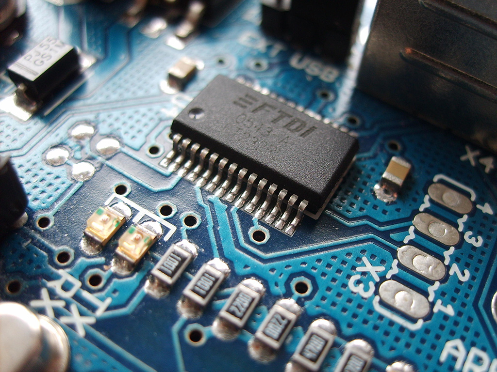
How to test IC using a multimeter?
Check whether there is a short circuit method of IC; Set the multimeter to continuous. Bridge all the pins on the IC side and connect them to one of the multimeter €™ s test probes. Test each IC pin with the remaining multimeter test probe: if there €™ continuity is in more than 50% of the pins, then the IC is likely to be short-circuited.
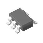
The latest precision comparator TLV9032QDDFRQ1, AEC-Q100, industrial temperature, standard leaded and leadless packages.
PCB circuit board design sequence
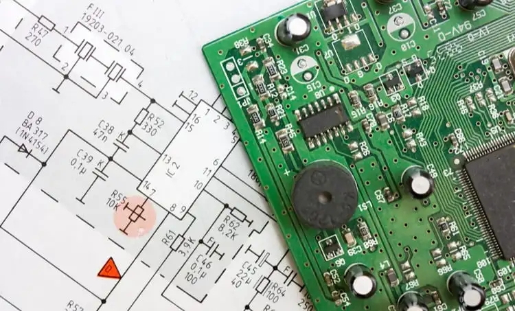
A PCB schematic is a desired design or blueprint. In the PCB layout design phase, the designer completes the wiring and placement of components. I used to work on a power electronics project where the control panel was connected vertically to the power circuit. Even when the controller PCB is working properly, the circuit board does not provide the desired output. After debugging, our team believes that there are some wiring errors in the power board. The results of PCB design services received from the service bureau where we outsourced work were poor. We had to redo the boards, which was a challenge and delayed the project. As a precaution, we blacklisted that particular service bureau from further projects. As we have learned, a poor PCB design service can have a negative impact on a project in many ways, as every stage of PCB design is critical to the success of the product. The following combination of my experience for you to summarize the PCB design sequence.
PCB conformal coatings and their types
Printed circuit boards are a core part of several devices and devices, so their structural and functional accuracy is critical to the functionality of the final product. This is why PCBS has a conformal coating, which is basically a polymer film applied to the board to protect the components mounted on it from any kind of contamination, dirt, etc. So, it's like an insulating layer. Conformal coatings come in many types according to their chemical composition. There are many advantages and types of PCB conformal coatings. This article discusses the details of conformal coating, its type, benefits, etc.
What is an X-ray inspection of PCB?
At the heart of most digital and electromechanical devices, printed circuit boards (PCBS) must be perfected in design, function, and so on. Their accuracy directly affects product functionality and enhancement. Therefore, flawless PCB design is of Paramount importance, with rigorous testing and inspection techniques at all stages throughout the manufacturing process. There are many types of testing techniques, such as manual, automatic optical inspection, X-ray inspection, etc., performed at specific stages. X-ray detection is a widely used detection technology for PCB and its components, which can find potential defects and improve quality.
Resistance and impedance in PCB layout
All electronic components have resistance and resistance, which together constitute impedance. Although we think the conductive trace on the PCB is a perfect conductor with zero resistance and zero reactance, this is not the case. Like the components on a circuit board, the materials that make up the board give it some resistance and resistance that determine the behavior of the signal. One goal of the designer in both domains (wave propagation and power) is to design a board to achieve an impedance or resistance goal, as both are affected by a particular layout choice. In this article, we will look at impedance and resistance and their impact on PCB layout.
LED PCB
LED PCB
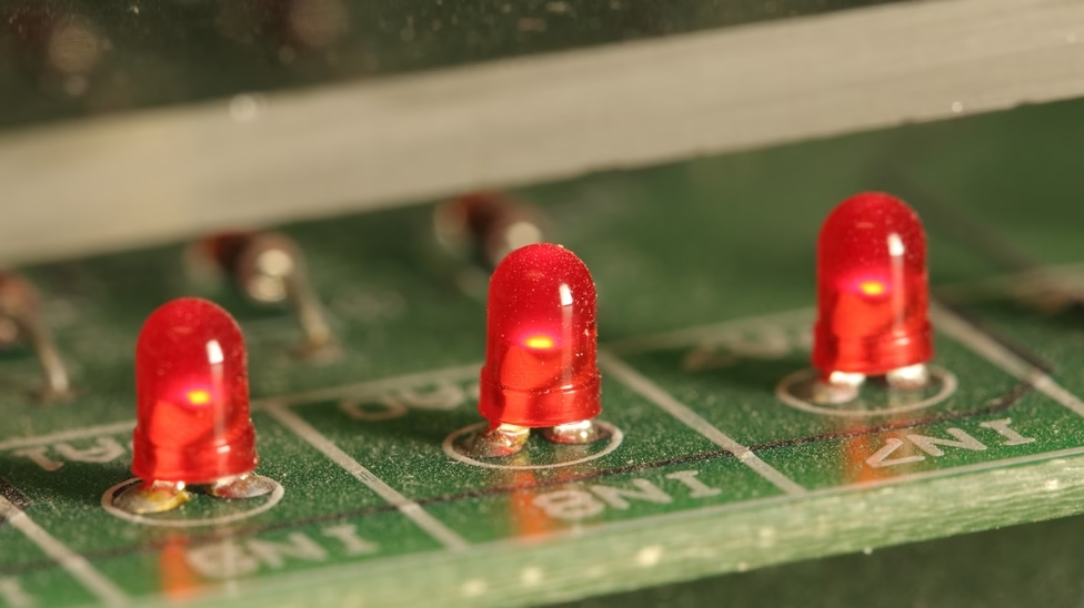
What is LED PCB? LED is short for a light-emitting diode, also known as a semiconductor diode. The LEDs are welded to a printed circuit board and fitted with a chip that generates light through an electrical connection. A heat sink and a ceramic base are used to attach the chips. There is no doubt that LED PCB is the core of LED lighting. An LED PCB is easy to generate a lot of heat, but it is difficult to cool with traditional methods. Metal core PCB is widely used in LED applications because of its strong heat dissipation ability, especially aluminum is often used in LED lamp PCB production. Typically, aluminum PCBS contains a thin layer of heat-conducting medium material that can transfer and dissipate heat much more efficiently than traditional rigid PCBS.
What’s The Difference Between Printed Circuit Board and Integrated Circuit Board?
What is a printed circuit board? Printed circuit board, also known as PCB, is the electrical connection provider of electronic components. It has a history of over 100 years. Its design is mainly layout design. The main advantages of using circuit boards are greatly reduced wiring and assembly errors and improved level of automation and production labor rate. According to the number of PCB, layers can be divided into a single board, double panel, four-layer board, six-layer board, and other multi-layer board. Let's look at printed circuit boards and integrated circuits.
Frequently Asked Questions about PCB
Almost every link and step in the PCB manufacturing process may have a variety of problems. Now we share some common bad phenomena of PCB as follows, hoping to learn from each other and make progress together.